Jingxugroup.net
Nano Res. 2011, 4(3): 290–296
Nano Res. 2011, 4(3): 290–296
DOI 10.1007/s12274-010-0081-x CN
Research Article
Hybrid Silicon-Carbon Nanostructured Composites as Superior
Anodes for Lithium Ion Batteries
Po-Chiang Chen1, Jing Xu1, Haitian Chen2, and Chongwu Zhou2 () 1 Mork Family Department of Chemical Engineering and Materials Science, University of Southern California, Los Angeles, CA 90089, USA2 Ming-Hsieh Department of Electrical Engineering, University of Southern California, Los Angeles, CA 90089, USA Received: 6 October 2010 / Revised: 13 November 2010 / Accepted: 13 November 2010 Tsinghua University Press and Springer-Verlag Berlin Heidelberg 2010
ABSTRACT
We have successfully fabricated a hybrid silicon–carbon nanostructured composite with large area (about
25.5 in2) in a simple fashion using a conventional sputtering system. When used as the anode in lithium ion
batteries, the uniformly deposited amorphous silicon (a-Si) works as the active material to store electrical energy,
and the pre-coated carbon nanofibers (CNFs) serve as both the electron conducting pathway and a strain/stress
relaxation layer for the sputtered a-Si layers during the intercalation process of lithium ions. As a result, the
as-fabricated lithium ion batteries, with deposited a-Si thicknesses of 200 nm or 300 nm, not only exhibit a high
specific capacity of >2000 mA·h/g, but also show a good capacity retention of over 80% and Coulombic efficiency
of >98% after a large number of charge/discharge experiments. Our approach offers an efficient and scalable
method to obtain silicon–carbon nanostructured composites for application in lithium ion batteries.
KEYWORDS
Amorphous silicon, carbon nanofibers, lithium ion batteries, hybrid nanostructured composite
1. Introduction
(1-D) nanostructures, have the advantages of high surface area (such as single-walled carbon nanotubes
In recent years, due to the depletion of fossil fuels
with a surface area of 300–600 m2/g) and short ion
and the increasing concern about environmental issues,
diffusion length, and have been viewed as components
interest in developing alternative energy sources and
for next-generation electrochemical energy conversion
devices, including solar cells, fuel cells, supercapacitors,
and storage devices [9–11]. For instance, TiO2–B nano-
and lithium ion batteries, has increased rapidly [1–6].
wires have been shown to have a higher specific
Among the above-mentioned energy conversion and
capacity than TiO2–B nanoparticle-based materials
storage devices, lithium ion batteries have been widely
when used as anodes in lithium ion batteries [11].
applied in both portable electronics and consumer
More recently, silicon (Si) nanostructures have been
electronics because of their high energy density, high
suggested to be one of the most promising anode
power density, and low fabrication cost. Most research
materials for lithium ion batteries and have attracted
efforts have been devoted to the synthesis of electrode
considerable attention because of their large theoretical
materials and the design of electrode structures [7, 8] by
gravimetric specific capacity of 4200 mA·h/g and
adapting nanostructured materials. One-dimensional
relatively low working potential at around 0.5 V vs.
Address correspondence to
[email protected]
Nano Res. 2011, 4(3): 290–296
Li/Li+ [12–20]. For instance, Chan et al. reported Si nanowires as anode materials and successfully de- monstrated an excellent specific capacity of 3124 mA·h/g during the first discharge process [12]. Further develop- ments include using homogeneous Si nanowires and hybrid Si core–shell nanowires, which have been demonstrated to deliver superior device performance as battery electrodes [21, 22]. For example, TiSi2–Si core–shell nanowires have been reported as one example of such novel Si nanostructure-based anodes [21]. The highly conductive core TiSi2 nanowires provide the electron conducting pathway and improve the battery power density by a factor of two. The TiSi2 nanowires also serve as a mechanical support and release the structural stress/strain associated with lithium ion insertion/extraction processes. In addition to core–shell nanowires, the preparation of nano- structured carbon–silicon composites seems to be another promising approach to solve the capacity retention problem [23–26]. However, synthesis of the above-mentioned materials usually requires a high temperature chemical vapor deposition process, and therefore alternative methods that can avoid a high- temperature process would be very interesting and attractive.
In this paper, we present a rather simple but efficient
approach to obtain hybrid Si-based nanostructured
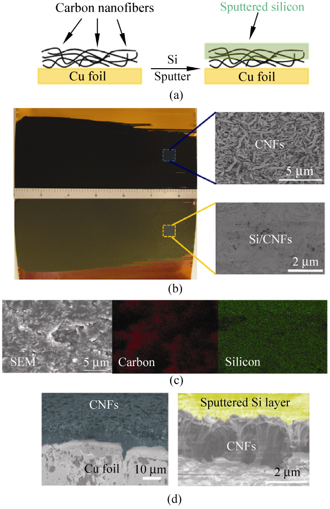
Figure 1 (a) Schematic diagram of sputtered silicon on CNF/copper
composites. By simply using a conventional sputtering
foil. (b) Photographs of CNFs on a copper foil before and after
system to deposit amorphous silicon (a-Si) on car-
200 nm silicon deposition. (c) Top-view SEM and EDX images
bonaceous materials pre-deposited on copper foil, we
of sputtered Si on CNFs. (d) Side-view of CNFs before and after
are able to obtain a hybrid Si-based nanostructured
500 nm silicon deposition
composite with a large area of 25.5 in2 and employ it as an anode in lithium ion batteries. In our design,
2. Experimental
carbon nanofibers (CNFs) are used as both mechanical support and electron conducting pathway. Different
The fabrication of Si hybrid nanostructured thin film
thicknesses of sputtered silicon were deposited on
electrodes began with the preparation of a CNF film
pre-deposited carbonaceous materials as the active
on copper foil. CNFs (Sigma-Aldrich) were deposited
materials to store electrical energy, as illustrated in
on copper (Cu) foil via a so-called slurry spreading
Fig. 1(a). These hybrid Si-based nanostructured
method, which has been widely adopted in the pre-
electrodes (Si/CNF) exhibit a high charge storage
paration of lithium ion battery electrodes. In brief,
capacity of 2528 mA·h/g and good cycling life up to a
CNFs were mixed with polyvinylidene fluoride (PVDF,
large number of charge/discharge cycles (>105 cycles).
10 wt%) in N-methylpyrrolidone (NMP) to form a
In addition, the as-fabricated batteries also show a
uniform slurry, and then spread onto a copper foil
Coulombic efficiency of 88% in the first cycle and over
using a stainless steel blade. The samples were installed
98% in the following cycles, which are comparable in a conventional sputtering system (Denton Discovery with results in the literature [25–28].
Sputtering System) for Si deposition. The loading
Nano Res. 2011, 4(3): 290–296
density of as-prepared CNF films was about 0.4 mg/cm2
to distinguish between carbon nanofibers (green) and
sputtered silicon (yellow). It can be seen that sputtered
Silicon deposition on CNFs was carried out in an
Si forms a uniform coating on CNFs, which is consistent
argon (Ar)-filled environment at room temperature,
with the image in Fig. 1(c).
with a deposition rate of 6 nm/min and varied
Electrochemical measurements of sputtered Si/CNF
deposition thicknesses of 100 nm, 200 nm, 300 nm, or
anodes were carried out with a battery testing system
500 nm. In order to compare the sputtered Si/CNF
(MSTAT, Arbin) and a potentiostat (Gamry Reference
anodes and Si electrodes, we sputtered 200 nm Si
600). The cyclic voltammetry (CV) profiles of sputtered
directly on to a Cu foil as the reference sample. The
Si/CNF anodes were obtained using the Si/CNF
as-prepared samples were then characterized by field-
electrode as the working electrode and Li foil as the
emission scanning electron microscopy (FE-SEM,
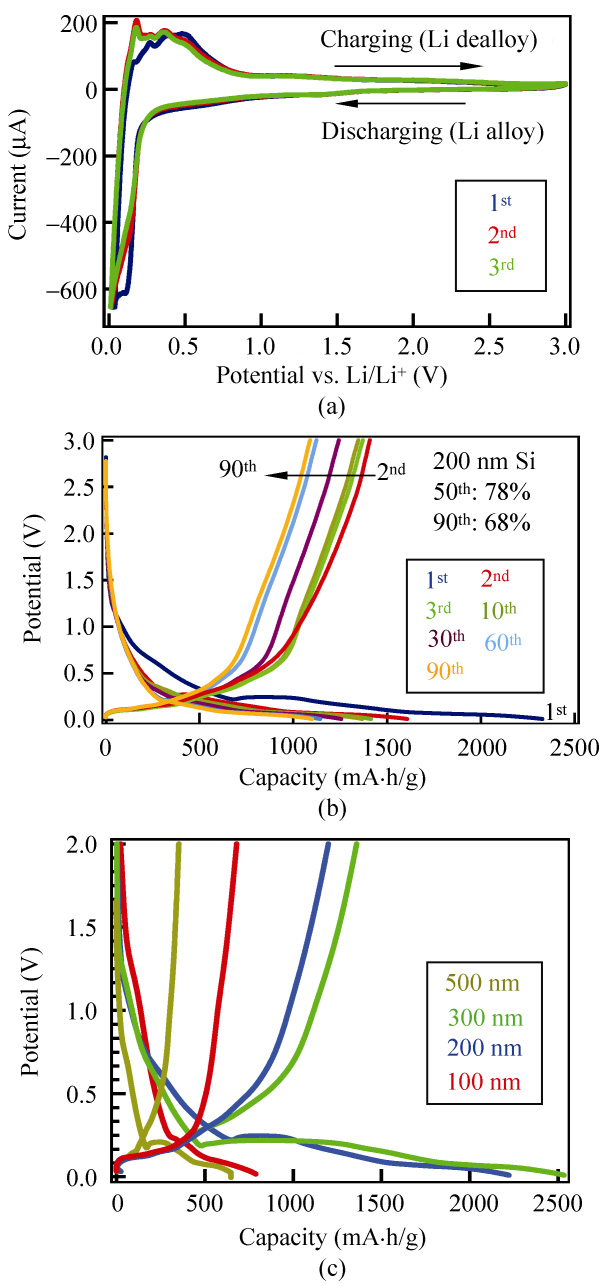
reference electrode. Figure 2(a) shows the first three CV
Hitachi S-4800) and energy-dispersive X-ray spectros-
curves of a sputtered Si/CNF anode with a deposited
copy (EDS, Jeol, JSM-7001F). CR2032 coin cells were
Si thickness of 200 nm, in a potential window between
assembled in an Ar-filled glove box by using the
0.01 V and 3.0 V, with a scan rate of 0.05 mV/s. Two
as-prepared Si/CNF anode as the working electrode
pairs of signature redox peaks of amorphous Si
and lithium metal foil as the counter electrode. The
can be found at around 0.18/0.03 V (reduction) and
electrolyte was 1 mol/L LiClO4 dissolved in a 1:1
0.50/0.30 V (oxidation) in the first cycling curve (blue
(weight ratio) mixture of ethylene carbonate (EC) and
line), which indicates the occurrence of Si–Li reactions
diethyl carbonate (DEC).
in the sputtered Si/CNF anode [28]. The shape of the first cycling curve differs from that of the second and third curves, where the sharp peak at 0.18 V disappears
3. Results and discussion
and the peaks at 0.50/0.30 V shift towards a lower
Figure 1(b) displays a photograph of a typical CNF
potential. The irreversible reaction in the first cycle
film on a Cu foil before (upper image) and after
can be attributed to the formation of a solid electrolyte
(lower image) the deposition of 500 nm Si. The Si
interface (SEI) layer or a phase transformation [29].
sputtered area is about 8.5 in × 3 in, making this method
However, the second and the third cycles match almost
a more efficient way to prepare large area Si-based
exactly, which implies the system has reached a steady
electrodes than the chemical vapor deposition (CVD)
state. No significant peaks related to CNFs [30] can
processes previously employed to prepare CNF-
be observed in Fig. 2(a). Overall, our sputtered Si/CNF
amorphous Si core–shell nanowire or Si nanowire
anodes display CV characteristics similar to amorphous
anodes [12, 22]. The zoomed-in SEM images in Fig. 1(b)
silicon [28], but different from carbon nanofibers [30],
are the top-view SEM images before and after the Si
suggesting the redox behavior of our anodes is
deposition. A uniform pre-deposited CNF thin film
dominated by the sputtered Si layer rather than the
on a the Cu foil can be clearly observed before Si
pre-coated CNF thin films.
deposition. After Si deposition, the CNFs were fully
Galvanostatic (GV) charge/discharge measurements
covered by a continuous Si film forming a hybrid
were used to determine the specific capacity (Csp),
Si/CNF nanostructured thin film electrode. In order to
and the Coulombic efficiency of the devices in a two-
study the interface between the CNFs and the sputtered
electrode configuration. Figure 2(b) shows the cycling
Si layer, we intentionally stretched a Si/CNF hybrid
performance of a 200 nm sputtered Si/CNF anode up
film electrode. In the top-view SEM image, shown in
to 95 cycles, with a constant charge/discharge current
Fig. 1(c), a uniform layered structure of a sputtered Si
of 0.05 A/g. In the initial state, the potential dropped
layer and CNFs can be clearly identified by the
to 0.22 V and maintained a flat plateau at around
contrast in the image. The thickness of the sputtered
0.25 V, before gradually decreasing to 0.01 V. The
Si layer shown in Fig. 1(c) is about 500 nm. Fig. 1(d)
stepped behavior of the discharge potential may
shows side-view SEM images of the electrodes before
result from the inactive nature of the Si film in the
and after silicon sputtering with artificial colors used
electrochemical reactions [29]. The capacity in the
Nano Res. 2011, 4(3): 290–296
that of commercial graphite anodes ( 90%) and better than that of lithium ion batteries made of single- crystalline Si nanowires ( 73%) [22]. The second discharge capacity decreased to 1608 mA·h/g, which can be attributed to the irreversible nature of Li–Si insertion and the formation of an SEI layer. After the first cycle, the reversible charge/discharge reactions were maintained over the subsequent 80 cycles.
To further understand the GV behavior of sputtered
Si/CNF anodes, we prepared Si/CNF anodes with different sputtering Si thicknesses of 100 nm, 300 nm, and 500 nm, and then performed GV measurements with the resulting Si/CNF anodes using a constant charge/discharge current of 0.05 A/g. The Si weight loadings were 5.8%, 15.5%, and 23.6% for 100 nm, 300 nm, and 500 nm sputtered Si, respectively. The first cycle for the Si/CNF anodes can be found in Fig. 2(c). As one can see, the voltage profile of 100 nm sputtered Si/CNF anode is quite different from that of 200 nm, 300 nm, and 500 nm sputtered Si/CNF anodes. The plateau at 0.22 V is short and not easy to observe, which indicates the discharge capacity might be contributed by the CNFs underneath the 100 nm sputtered Si, and the discharge capacity is only 786 mA·h/g. On the other hand, with more Si deposition on the CNFs, both 300 nm and 500 nm sputtered Si/CNF anodes exhibit prolonged plateaus at around 0.22 V. The 300 nm sputtered Si/CNF anode shows the highest discharge capacity of 2528 mA·h/g, which is more than three-times that of the 100 nm sputtered Si/CNF anode. However, the discharge capacity of 500 nm sputtered Si/CNF anode is only 648 mA·h/g. In con-
clusion, our observations indicate that 200 nm and
Figure 2 (a) Cyclic voltammograms for 200 nm Si on CNFs from
300 nm films offer better performance than 500 nm
0.01 to 3.0 V. The first three cycles are shown. (b) Voltage profile for
films. More experiments are required to understand
first 90 cycles of the 200 nm sputtered Si/CNF anode at a constant charge/discharge current of 0.05 A/g. (c) Voltage profile for the
these phenomena.
first cycle of the 100 nm, 200 nm, 300 nm, and 500 nm Si/CNF
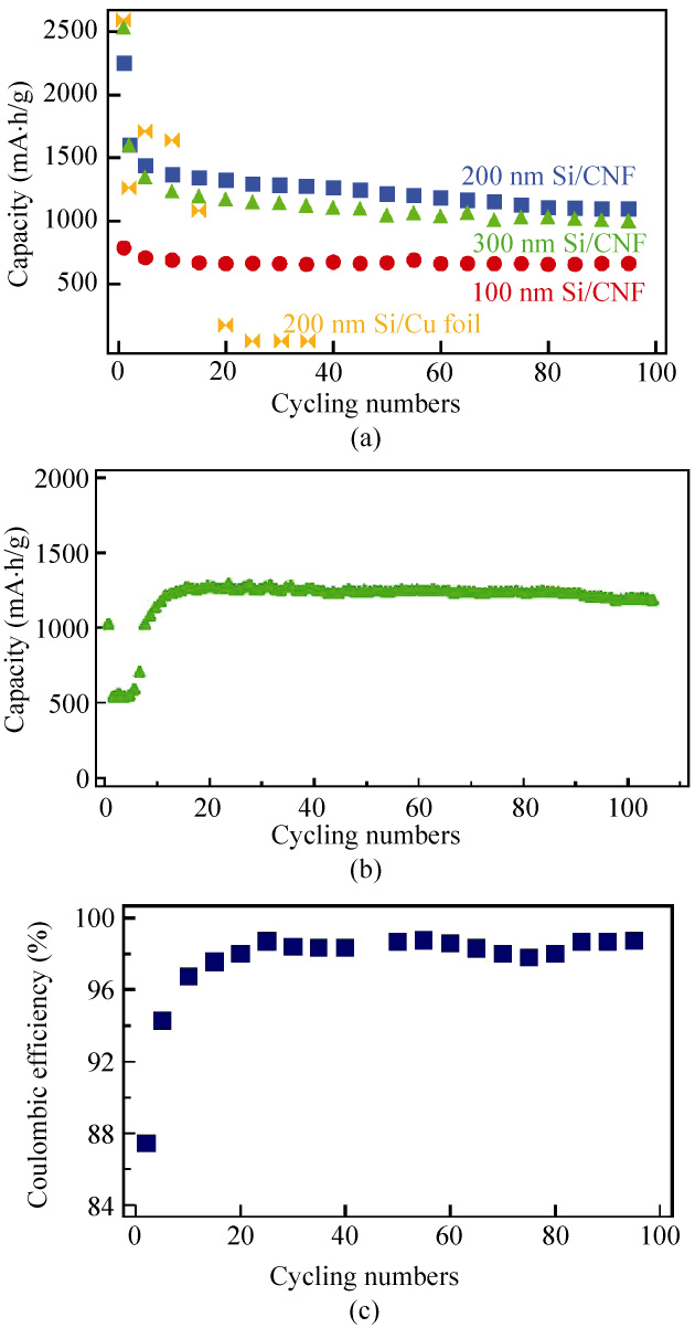
Figure 3(a) shows plots of the capacity retention
anodes at a constant charge/discharge current of 0.05 A/g
versus cycling number for electrodes with different thicknesses of sputtered Si (100 nm, 200 nm, and
first discharge process of sputtered Si/CNF anodes
300 nm). The weight densities for 100 nm, 200 nm and
was about 2320 mA·h/g. Our results are better than
300 nm sputtered Si are 0.02 mg/cm2, 0.049 mg/cm2
those reported for an amorphous Si microbattery
and 0.071 mg/cm2, respectively. When calculating the
( 650 mA·h/g), and close to those reported for CNF–
capacity, we have included the weight of the CNFs.
amorphous Si core–shell nanostructured electrodes.
As one can see, all Si/CNF anodes displayed good
In addition, the Coulombic efficiency of our devices
capacity retention, especially the 100 nm Si/CNF anode
in the first cycle is about 88%, which is comparable to
( 84% after 95 cycles). This is probably because there
Nano Res. 2011, 4(3): 290–296
is more space for volume expansion than in the thicker sputtered Si samples. For 200 nm Si/CNF anodes, the capacity retention up to the 50th cycle ( 80%) is close to values reported in the literature. Good capacity retention was also observed even at a higher charge/ discharge rate (C/4). In this case, as shown in Fig. 3(b), the 300 nm Si/CNF anode exhibited a high specific capacity up to 1200 mA·h/g after 105 cycles, corres- ponding to over 90% capacity retention. In the initial stage of the cycle tests, a reduced capacity was obser- ved, and after about 10 cycles, the capacity recovered to about 1200 mA·h/g. Similar observations have reported by Takamura et al. [31, 32] and can be understood in terms of the Si film initially being very compact and unable to accept a large amount of Li, but after repeated Li insertion/extraction, the film structure underwent changes enabling it to accept more Li. To highlight the advantage of our Si/CNF anodes, we directly sputtered 200 nm Si on Cu foil (Si/Cu) and carried out GV measurements as a comparison. As expected, the Si/Cu anode showed extremely poor capacity retention, which can be attributed to the huge volume expansion after Li ion insertion/extraction. After 20 cycles, there was almost no measurable capacity from the anode, indicating a total loss of active material. We also investigated the Coulombic efficiency of our devices and, as an example, the results for the 200 nm sputtered Si/CNF anodes are shown in Fig. 3(c). The cell exhibited a good first cycle of Coulombic efficiency of 88%. The Coulombic efficiency in the second cycle increased to 93% and a
very high Coulombic efficiency between 98%–99% was
Figure 3 (a) Discharge capacity of 100 nm, 200 nm, and 300 nm
sputtered Si/CNF anodes, and 200 nm Si/Cu anodes at a current
maintained over the next 80 cycles. Subsequently, the
rate C/10. (b) Discharge capacity of 300 nm sputtered Si/CNF
discharge capacities faded a little but remained at
anodes at a current rate C/4. (c) Coulombic efficiency of a 200 nm
70% up to 90 cycles (relative to the second cycle).
sputtered Si/CNF anode
Such good capacity retention was not observed for the 200 nm electrode, but also for 100 nm and 300 nm
the Si surface after 95 cycles appears rough, as a
sputtered Si/CNF anodes.
consequence of the lithiation/delithiation processes.
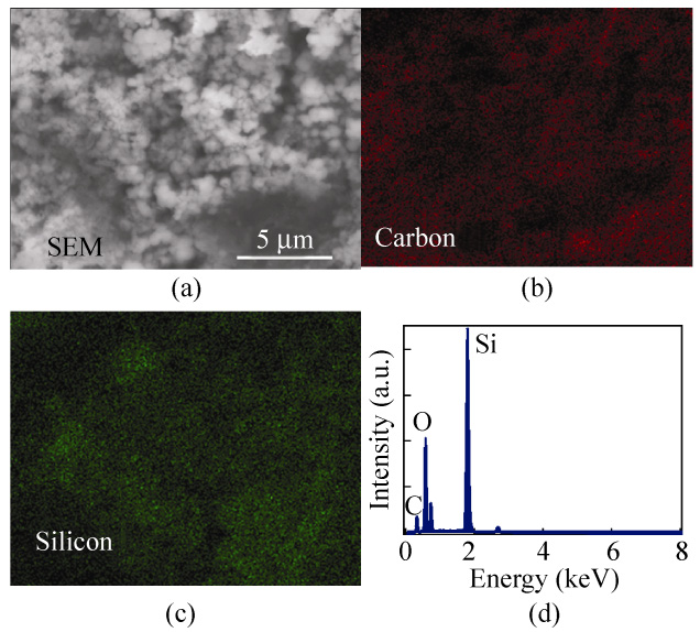
In order to study any variation in chemical com-
Figures 4(b) and 4(c) show EDS images of the sputtered
position of our sputtered Si/CNF anodes after the
Si/CNF electrodes. The red color represents carbon
cycling experiments, EDS was carried out and the
atoms and the green color indicates the presence of
results are shown in Fig. 4. The SEM image of a 200 nm
silicon atoms. The EDS mapping strongly suggests
sputtered Si/CNF anode after 95 charge/discharge
that the sputtered Si layer is still well coated on CNFs
cycles (Fig. 4(a)) clearly shows that there is still good
and has a strong adhesion with them, even after a
adhesion between Si and the substrate. In addition,
large number of cycling experiments. Although the
compared with the pristine surface shown in Fig. 1(b),
sputtered Si film was broken into small grain domains
Nano Res. 2011, 4(3): 290–296
compared to conventional batteries, the total weight of our devices is reduced because binder materials are not required. Si/CNF lithium ion batteries are expected to find applications in portable electronics and electrical vehicles.
We acknowledge financial support from the National Science Foundation (CCF 0726815 and CCF 0702204).
References
[1] Winter, M.; Brodd, R. J. What are batteries, fuel cells, and
supercapacitors. Chem. Rev. 2004, 104, 4245–4270.
[2] Kang, K.; Meng, Y. S.; Bréger, J.; Grey, C. P.; Ceder, G.
Figure 4 (a) SEM image of 200 nm sputtered Si/CNF anodes after
Electrodes with high power and high capacity for rechargeable
95 cycles of charge/discharge measurements. (b) EDS image of carbon atoms. (c) EDS image of silicon atoms. (d) EDS spectrum
lithium batteries. Science 2006, 311, 977–980.
of 200 nm sputtered Si/CNF anodes after 95 cycles of chargeg/
[3] Yoon, J.; Baca, A. J.; Park, S. -I.; Elvikis, P.; Geddes, J. B.,
dischare measurements
Ⅲ; Li, L.; Kim, R. H.; Xiao, J.; Wang, S.; Kim, T. -H.; Motala, M. J.; Ahn, B. Y.; Duoss, E. B.; Lewis, J. A.; Nuzzo,
after lithiation/delithiation processes, as shown in
R. G.; Ferreira, P. M.; Huang, Y.; Rockett, A.; Rogers, J. A.
Fig. 4(c), the good capacity retention and the EDS
Ultrathinsilicon solar microcells for semitransparent, mech-
results indicate that each grain domain maintained
anically flexible and microconcentratormoduledesigns. Nat.
Mater. 2008, 7, 907–915.
its strong adhesion with the underlying CNFs. A
[4] Armand, M.; Tarascon, J. -M. Building better batteries.
similar observation was recently reported by Rong et
Nature 2008, 451, 652–657.
al. [33], who concluded that a Si film can form a convex
[5] Boettcher, S. W.; Spurgeon, J. M.; Putnam, M. C.; Warren,
morphology with a cone-shaped "lattice" on the surface
E. L.; Turner-Evans, D. B.; Kelzenberg, M. D.; Maiolo J. R.;
which can be squeezed to release the internal stress.
Awater, H. A.; Lewis, N. S. Energy-conversion properties
Figure 4(d) shows a typical EDS spectrum of the
of vapor–liquid–solid-grown silicon wire-array photocathodes.
sputtered Si/CNF electrodes. The atomic ratio of C:Si is
Science 2010, 327, 185–187.
estimated to be 9:1.
[6] Long, J. W.; Dunn, B.; Rolison, D. R.; White, H. S. Three-
dimensional battery architectures. Chem. Rev. 2004, 104,
4463–4492.
4. Conclusions
[7] Liu, J.; Cao, G.; Yang, Z.; Wang, D.; Dubois, D.; Zhou, X.;
We have developed a simple and efficient way to obtain
Graff, G. L.; Pederson, L. R.; Zhang, J. -G. Oriented nano- structures for energy conversion and storage. ChemSusChem
hybrid nanostructured thin film electrodes for use in
2008, 1, 676–697.
lithium ion batteries. Our hybrid nanostructured
[8] Simon, P.; Gogotsi, Y. Materials for electrochemical capacitors.
Si/CNF anodes exhibited superior device performance
Nat. Mater. 2008, 7, 845–854.
to those for materials used in previous studies, in
[9] Jiang, C.; Hosono, E.; Zhou, H. E. Nanomaterials for lithium
terms of both specific capacity and cycle life. The
ion batteries. Nano Today 2006, 1, 28–33.
superior performance can be attributed to (1) the
[10] Poizot. P.; Laruelle, S.; Grugeon, S.; Dupont, L.; Tarascon,
utilization of CNFs, which provide a good strain/stress
T. -M. Nano-sized transition-metal oxides as negative-electrode
relaxation layer and a conductive electron pathway,
materials for lithium-ion batteries. Nature 2000, 407, 496–499.
and (2) the sputtered amorphous Si, which contributes
[11] Arico, A. S.; Bruce, P.; Scrosati, B.; Tarascon, T. -M.;
high specific capacity to the half cells. In addition,
Schalkwijk, W. V. Nanostructured materials for advanced
Nano Res. 2011, 4(3): 290–296
energy conversion and storage devices. Nat. Mater. 2005, 4,
high energy-density lithium ion batteries. J. Power Sources
2010, 195, 5052–5056.
[12] Chan, C. K.; Peng, H.; Liu, G.; Mcilwrath, K.; Zhang, X. F.;
[24] Wang, W.; Kumta, P. N. Nanostructured hybrid silicon/carbon
Huggins, R. A.; Cui, Y. High-performance lithium battery
nanotube heterostructures: Reversible high-capacity lithium-ion
anodes using silicon nanowires. Nat. Nanotechnol. 2008, 3,
anodes. ACS Nano 2010, 4, 2233–2241.
[25] Luo, Z.; Fan, D.; Liu, X.; Mao, H.; Yao, C.; Deng, Z. High
[13] Park, M. H.; Kim, M. G.; Joo, J.; Kim, K.; Kim, J.; Ahn, S.;
performance silicon carbon composite anode materials for
Cui, Y.; Cho, J. Silicon nanotube battery anodes. Nano Lett.
lithium ion batteries. J. Power Sources 2009, 189, 16–21.
2009, 9, 3844–3847.
[26] Saint, J.; Morcrette, M.; Larcher, D.; Laffont, L.; Beattie, S.;
[14] Song, T.; Xia, J.; Lee J. -H.; Lee, D. H.; Kwon, M. -S.; Choi,
Peres, J. -P.; Talaga, D.; Couzi, M.; Tarascon, J. -M. Towards
J. -M.; Wu, J.; Doo, S. K.; Chang, H.; Park, W. I.; Zang,
a fundamental understanding of the improved electrochemical
D. S.; Kim, H.; Huang, Y.; Hwang, K. -C.; Rogers, J. A.;
performance of silicon–carbon composites. Adv. Funct. Mater.
Paik, U. Arrays of sealed silicon nanotubes as anodes for
2007, 17, 1765–1774.
lithium ion batteries. Nano Lett. 2010, 10, 1710–1716.
[27] Cui, L. F.; Ruffo, R.; Chan, C. K.; Peng, H. L.; Cui, Y.
[15] Cho, J. Porous Si anode materials for lithium rechargeable
Crystalline-amorphous core–shell silicon nanowires for
batteries. J. Mater. Chem. 2010, 20, 4009–4014.
high capacity and high current battery electrodes. Nano Lett.
[16] Kim, H.; Han, B.; Choo J.; Cho, J. Three-dimensional porous
2009, 9, 491–495.
silicon particles for use in high-performance lithium secondary
[28] Baranchugov, V.; Markevich, E.; Pollak, E.; Salitra, G.;
batteries. Angew. Chem. Int. Ed. 2008, 47, 10151–10154.
Aurbach, D. Amorphous silicon thin films as a high capacity
[17] Kim, H.; Cho, J. Superior lithium electroactive mesoporous
anodes for Li-ion batteries in ionic liquid electrolytes.
Si@carbon core–shell nanowires for lithium battery anode
Electrochem. Commun. 2007, 9, 796–800.
material. Nano Lett. 2008, 8, 3688–3691
[29] Lee, K. -L.; Jung, J. -Y.; Lee, S. -W.; Moon, H. -S.; Park,
[18] Kim, H; Seo, M.; Park, M. -H.; Cho, J. A critical size of
J. -W. Electrochemical characteristics and cycle performance
silicon nano-anodes for lithium rechargeable batteries. Angew.
of LiMn2O4/a-Si microbattery. J. Power Sources 2004, 130,
Chem. Int. Ed. 2010, 49, 2146–2149.
[19] Cui, L. F.; Hu, L. B.; Choi, J. K.; Cui, Y. Light-weight
[30] Zaghib, K.; Tatsumi, K.; Abe, H.; Ohsaki, T.; Sawada, Y.;
free-standing carbon nanotube–silicon films for anodes of
Higuchi, S. Optimization of the dimensions of vapor-grown
lithium ion batteries. ACS Nano 2010, 4, 3671–3678
carbon fiber for use as negative electrodes in lithium-ion
[20] Choi, J. W.; Hu, L. B.; Cui, L. F.; McDonough, J. R.; Cui,
rechargeable cells. J. Electrochem. Soc. 1998, 145, 210–215.
Y. Metal current collector-free freestanding silicon-carbon
[31] Takamura, T.; Ohara, S.; Uehar, M.; Suzuki, J.; Sekine, K.
1D nanocomposites for ultralight anodes in lithium ion
A vacuum deposited Si film having a Li extraction capacity
batteries. J. Power Sources 2010, 195, 8311–8316
over 2000 mA·h/g with a long cycle life. J. Power Sources
[21] Zhou, S.; Liu, Z.; Wang, D. Si/TiSi2 heteronanostructures
2004, 129, 96–100.
as high-capacity anode material for Li ion batteries. Nano
[32] Ohara, S.; Suzuki, J.; Sekine, K.; Takamura, T. A thin film
Lett. 2010, 10, 860–863.
silicon anode for Li-ion batteries having a very large
[22] Cui, L. F.; Yang, Y.; Hsu, C. M.; Cui, Y. Carbon–silicon
specific capacity and long cycle life. J. Power Sources 2004,
core–shell nanowires as high capacity electrode for lithium
136, 303–306.
ion batteries. Nano Lett. 2009, 9, 3370–3374.
[33] Rong, J. P.; Masarapu, C.; Ni, J.; Zhang, Z. J.; Wei, B. Q.
[23] Wang, L.; Ding, C. X.; Zhang, L. C.; Xu, H. W.; Zhang, D. W.;
Tandem structure of porous silicon film on single-walled carbon
Cheng, T.; Chen, C. H. A novel carbon–silicon composite
nanotube macrofilms for lithium-ion battery applications.
nanofiber prepared via electrospinning as anode material for
ACS Nano 2010, 4, 4683–4690.
Source: https://jingxugroup.net/papers/006.pdf
Prevention and the of breast cancerA report commissioned by GE Healthcare, authored by Bengt Jönsson and Nils Wilking Br grow cure begins cases Blood skin nodes Among although familiar screening malignant organs seven About the authors Professor Bengt Jönsson
Single-pass CO2-laser skin resurfacing in combination with cold air cooling. Efficacy and patient satisfaction of a prospective side-by- side study Christian Raulin, Hortensia Grema, Laserklinik Karlsruhe, Karlsruhe, Germany Word count: 1998 Correspondence address: Christian Raulin, M.D. Laserklinik Karlsruhe Kaiserstr. 104 Germany 76133 Karlsruhe www:


